

Semiconductor companies embrace digitalization and leverage the comprehensive digital twin
The semiconductor industry is on track to hit a $1 trillion valuation by 2030. While surging demand drives impressive growth, many chipmakers face heavy financial burden from rising fabrication (fab) construction and chip design costs. Building a new fab averages about $19 billion, while individual chip designs routinely require a $1 billion investment.
As software-defined products (SDPs) increasingly power modern hardware, they are becoming central to the evolution of the semiconductor industry. To make custom part fabrication for SDPs affordable, semiconductor companies must embrace digitalization and leverage the comprehensive digital twin (cDT) across both design and manufacturing.
Taking advantage of virtual space
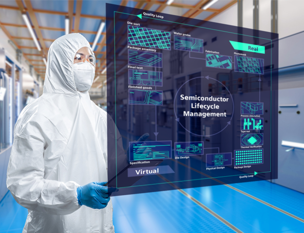
Bridging the gap between isolated engineering and manufacturing teams, the physics-based comprehensive Digital Twin (cDT) is engineered to solve tomorrow’s software-enabled semiconductor challenges. By weaving together mechanical, electrical, electronic software, and production workflows into a unified platform, the cDT ensures that cross-functional teams can engage and collaborate seamlessly from the earliest stages.
Specifically, the cDT bridges the physical and digital worlds through consistent digital models spanning the entire product, production lifecycle, and supply chain. Engineers can now accomplish more virtually before committing to costly physical prototypes or commissioning an expensive fab. This yields higher-quality products while satisfying aggressive cost, timeline, and sustainability targets.
In the design phase, this “shift-left” approach provides a physics-based virtual environment where teams can create, simulate, and refine products rapidly. Virtual iterations consume virtually no physical resources outside of engineering brainpower, unlocking a broader design space. In production, companies can virtually evaluate and optimize assembly lines, commission machinery, and analyze entire factory networks to boost speed, efficiency, and sustainability. The system analyzes real fab data to feed advanced AI metrics.
Managing the friction between hardware and software teams—while balancing mechanical constraints and manufacturing requirements—is a major hurdle for the semiconductor ecosystem. The comprehensive digital twin tackles this head-on, delivering core operational benefits including:
- Faster new product introductions: virtualizing the design phase speeds up prototype creation, which will become even more important as the quest to pursue “More than Moore” normalizes advanced packaging.
- Faster path to higher yields: simulating the production process makes enhancing IC quality easier, enabling workers to enact changes dynamically on the shop floor to quickly achieve higher yields for greater profitability.
- Traceability and zero defects: it is now possible to update the digital twin of both the product and production in tandem with their real-world counterparts, enabling manufacturers to diagnose issues and detect anomalies before they happen in the pursuit of zero defects.
- Dynamic planning and scheduling: since the digital twin provides an adaptive comparison between the physical and digital counterparts, it can detect disturbances within systems and trigger rescheduling in a timely manner.
Simplifying for better gains
Next-generation semiconductor development demands serious financial commitment. Yet, chipmakers cannot afford to stall; they must continually engineer cutting-edge designs backed by increasingly sophisticated fabrication technologies to power tomorrow’s software-defined products. To successfully navigate this fast-evolving ecosystem, semiconductor businesses will increasingly depend on the comprehensive digital twin.
By deploying the cDT to virtualize end-to-end process designs for software-enabled goods, companies can simulate everything from raw conceptual sketches and manufacturing protocols right down to final product integration. This capability dramatically shrinks development cycles and elevates final market outcomes. Ultimately, successfully integrating these workflows and maximizing the true value of data will pave the semiconductor industry’s path to the $1 trillion milestone.
(Source: Siemens)
Read more:
- Arm finds success with Siemens Aprisa place-and-route
- Top 6 reasons to choose IC design solutions from Siemens EDA