


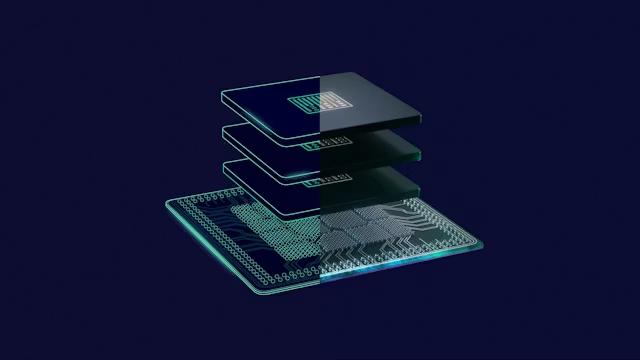
Six Key Trends Redefining 3D IC Packaging in the AI Era
The semiconductor industry is entering an era in which continued performance scaling can no longer rely solely on transistor shrinkage.
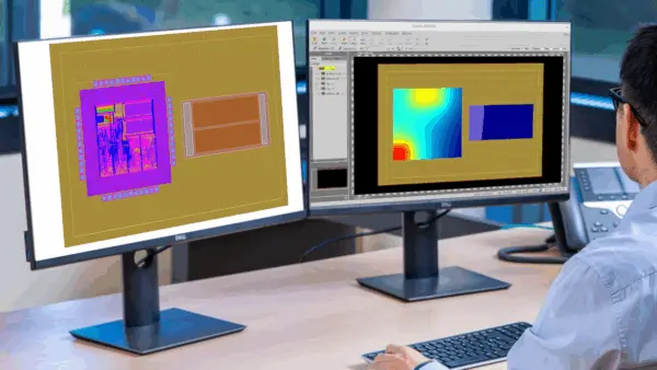
Thermal management in 3D IC: Challenges, modeling and design strategies
Thermal management in 3D ICs directly affects design performance, reliability and lifetime. As multiple dies are stacked within a smaller
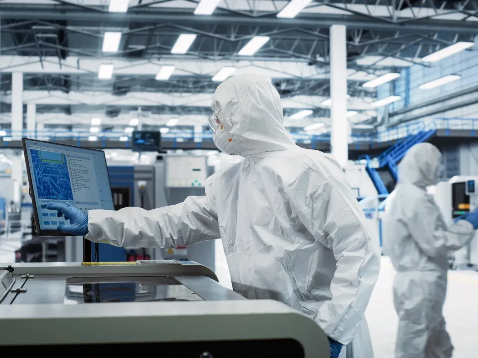
Discover how comprehensive digital twins tranform semiconductors
The semiconductor industry is on track to hit a $1 trillion valuation by 2030. While surging demand drives impressive growth,