
Explore Siemens Xpedition: Features, Benefits, and Editions
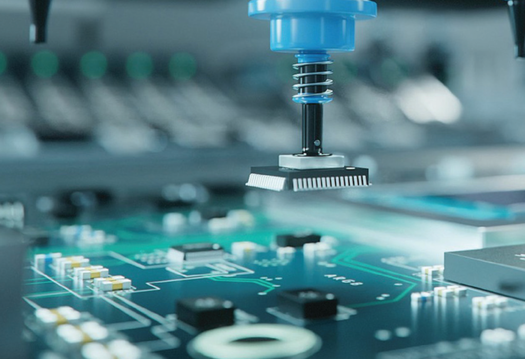
Xpedition is Siemens EDA’s advanced printed circuit board design solution (PCB – Printed Circuit Board), developed to support the entire

How to drive routing automation with human intelligence
The rapid pace of electronics innovation demands PCB design workflows that combine speed with decision quality.
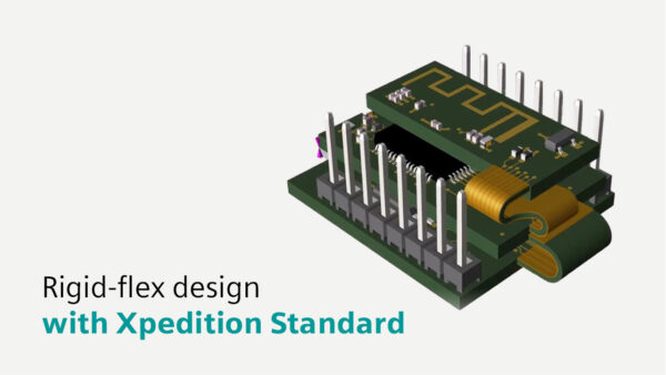
Rigid-flex PCB design with Xpedition Standard
When innovation demands flexibility, and space is limited, rigid-flex PCBs make it possible to reimagine product design across industries, from