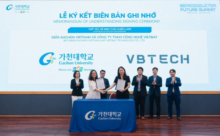
VBTECH signs MOU with Gachon University Vietnam at Semiconductor Future Summit
On April 11, 2026, within the framework of the Semiconductor Future Summit – “Inside the Chip – Inside the Future”
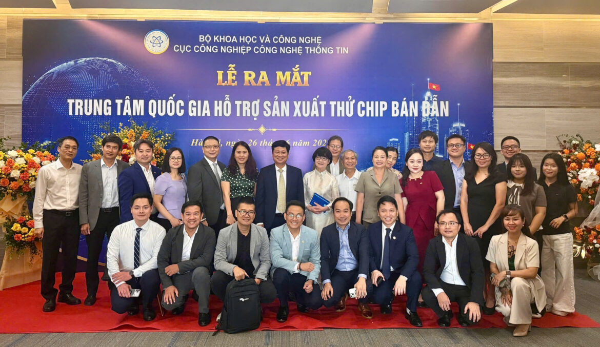
VBTECH participates in the Launch of Vietnam’s National Semiconductor MPW Support Center (VNMPW/CC)
On June 26, 2026, CEO of VBTECH, Mrs Dam Thi Hong Lan attended the launch ceremony of the Vietnam National
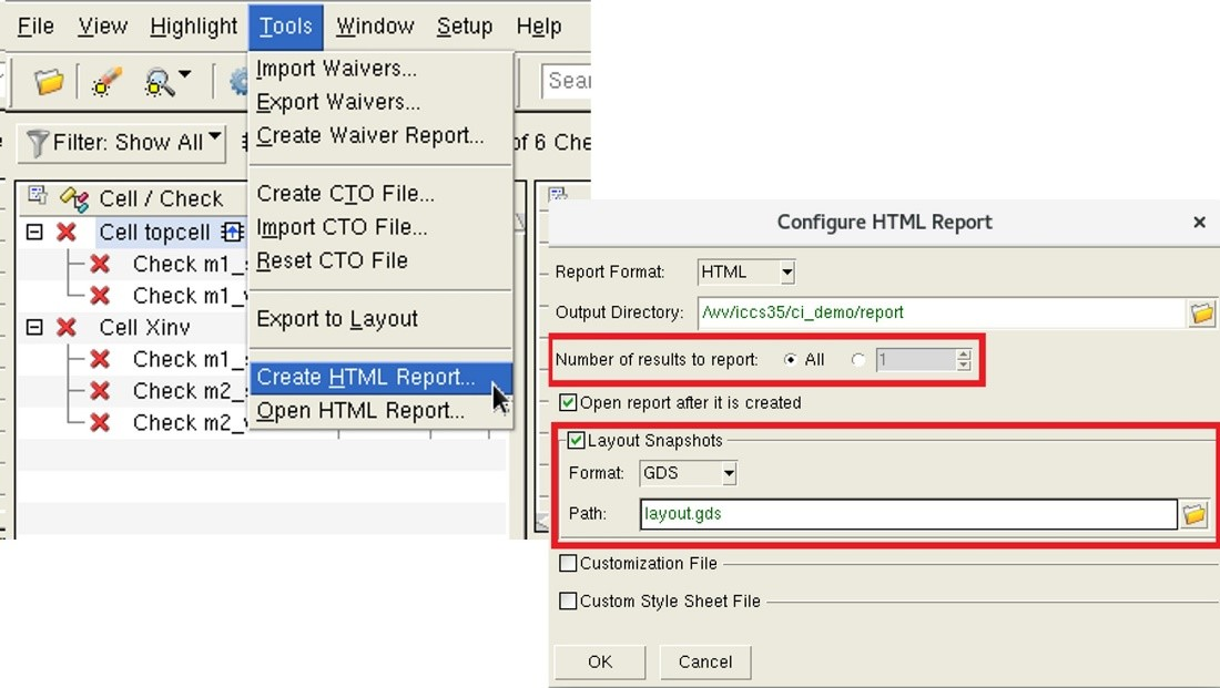
A new physical verification reporting solution smooths the on-time tapeout effort
In the intricate world of system-on-chip (SoC) development, Physical Verification (PV) reports serve as vital checkpoints throughout the iterative final