Research and Experience center for design IC
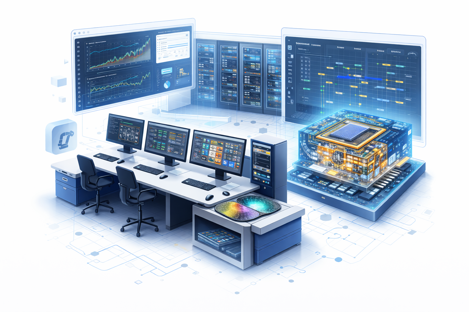
The Research and Experience Center for IC Design, powered by Siemens EDA solutions, provides a comprehensive environment for semiconductor design, verification, and manufacturing readiness. The center supports the full IC development flow—from front-end design and functional verification to physical implementation and tape-out preparation.
Equipped with advanced EDA tools, the center enables engineers, researchers, and students to gain hands-on experience in chip design, ensuring compliance with industry standards and optimizing performance. It also serves as a platform for innovation, training, and collaboration, helping develop high-quality talent and accelerate the growth of the semiconductor ecosystem.
Related Information
Find the Right Solution for Your Business
Get in Touch with Our Experts for a Free Consultation on EDA and CAD/CAM/CAE/CNC/PDM/PLM Solutions.
Contact us