

Thermal management in 3D ICs directly affects design performance, reliability and lifetime. As multiple dies are stacked within a smaller space, power density increases and heat dissipation paths become more complex. Thermal analysis at the architectural stage helps engineers identify hotspots, evaluate design options and reduce costly changes late in the development cycle.
For projects involving stacked dies, advanced packaging or heterogeneous integration, analyzing each die separately is not enough. Design teams need to consider the interactions between the chip, package and cooling system to determine the operating limits of the complete assembly.
What is thermal management in 3D ICs?
Thermal management in 3D ICs involves analyzing, predicting and controlling temperatures across vertically stacked dies to meet product performance, reliability and lifetime targets.
Compared with 2D IC designs, heat in a 3D structure may need to pass through multiple silicon layers, bonding layers and material interfaces before reaching a heat sink. The thermal resistance of these layers affects heat dissipation and the formation of localized hotspots.
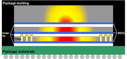
Figure 1. Illustration of thermal hotspots in a 3D IC.
If heat generation exceeds cooling capacity, the design may need to operate at a lower frequency to stay within allowable temperatures. High temperatures can also accelerate component aging. Thermal requirements therefore need to be considered throughout architecture selection, package design and system integration.
Why is thermal management more challenging in 3D IC designs?
High power density increases the risk of hotspots
Stacking logic, memory and other functional dies increases integration density but also concentrates heat sources within a smaller volume. Even when total power is comparable to that of a 2D design, local heat flux can be higher.
Design teams therefore need to consider both total power and the locations of high-power regions. A configuration that meets overall power limits can still develop hotspots that exceed allowable temperatures.
Multiple material layers create more complex heat dissipation paths
In a stacked-die structure, heat from dies farther from the heat sink may need to travel through multiple layers and material interfaces. Heat flow direction depends on the package structure, heat sink location and cooling conditions; it is not necessarily from top to bottom.
Interfaces along the heat flow path add thermal resistance, affecting peak temperatures and temperature differences between regions. Stack order and die placement should therefore be evaluated together with the cooling approach from the outset.
Dies are thermally coupled
Heat generated by one die can raise the temperature of neighboring dies. This thermal coupling means that even a relatively low-power die can be affected by a heat source in an adjacent layer.
Analyzing dies individually may miss these interactions. Evaluating the entire stack helps identify hotspot locations and system-level thermal limits more accurately.
Factors that govern heat flow in 3D ICs
Heat propagates through silicon, bonding layers, electrical interconnects and package components. Heat transfer efficiency depends on material thermal conductivity, interface thermal resistance and the boundary conditions of the model.
Through-silicon vias (TSVs) provide electrical connectivity and influence heat transfer within the stack. Their impact depends on their materials, density and locations relative to heat sources. TSVs should therefore be evaluated within the overall model rather than assuming that adding more TSVs always improves cooling.
Bonding layers and thermal interface materials (TIMs) affect heat transfer between surfaces. Thermal resistance at these interfaces can create bottlenecks, even when other components conduct heat effectively.
The package structure and cooling system determine how heat is removed from the die stack. Optimizing an individual layer may not lower temperatures across the system if the bottleneck remains in the package substrate, contact interfaces or heat sink.
How should thermal modeling be implemented for 3D ICs?
Start during architecture selection
Early in the design process, simplified thermal models help compare stack configurations, power distributions and package structures. The goal is to identify thermal trends and high-risk options before physical design constraints become fixed.
As more data becomes available, the design team refines the model with detailed geometry, material properties and boundary conditions. This approach maintains continuity from architectural exploration through final design verification and approval (signoff).
Combine steady-state and transient analysis
These two analysis methods answer different questions and should be selected according to the operating scenarios being evaluated.
| Method | Purpose | Use cases |
| Steady-state analysis | Evaluate temperature distribution when the workload and boundary conditions are maintained until thermal equilibrium is reached | Compare stack configurations and assess heat dissipation under sustained workloads |
| Transient analysis | Track temperature changes over time | Evaluate varying workloads or activity shifting between dies |
Steady-state analysis does not fully capture how temperatures rise and fall as workloads change. Adding transient analysis helps design teams better understand thermal responses under dynamic operating conditions.
Maintain consistent data from chip to system
Assumptions about power, die placement, materials and cooling conditions need to be updated consistently as the design evolves. If different teams use different assumptions, analysis results may be difficult to compare and may not reflect the final configuration accurately.
A chip–package thermal co-design workflow connects architectural decisions with detailed analysis. This allows engineers to track the impact of each change and evaluate alternatives using a consistent data foundation.
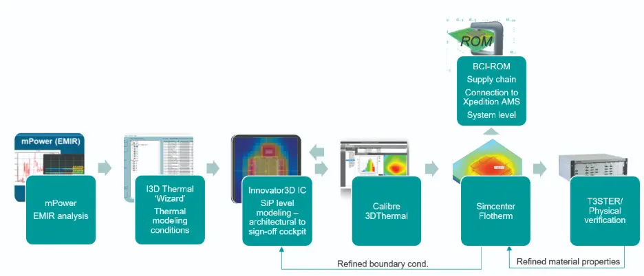
Figure 2. Siemens’ integrated thermal analysis flow for 3D ICs.
Effective thermal management strategies for 3D IC designs
Optimize stack order and die placement
In many configurations, placing high-power dies closer to the heat sink can shorten heat flow paths and reduce peak temperatures. However, this choice must be balanced against electrical connectivity, layout and packaging requirements.
Early evaluation gives design teams more options before architectural changes become complex or expensive.
Improve bonding layers and thermal interfaces
Thermal interface materials and bonding layers can contribute significantly to total thermal resistance. Optimizing these components helps improve heat dissipation paths throughout the stack.
Design teams should include interface properties in their models early and update them using actual material data and package configurations. Preliminary assumptions should not remain unchanged until final verification.
Evaluate thermal, electrical and mechanical behavior together
A thermally favorable option may affect electrical performance, mechanical stress or package implementation. Designs therefore need to be evaluated against multiple criteria to select an option that meets product objectives.
No single cooling technique is suitable for every 3D IC. Decisions about advanced cooling should be based on power density, stack structure and system operating limits.
Integrate thermal analysis throughout the design flow
Embedding thermal analysis into design stages helps engineers identify risks while they can still change the architecture, materials or layout. Continuing to assess thermal behavior as the model becomes more detailed helps reduce discrepancies between early evaluations and the final design.
This approach supports informed decisions, reduces late-stage design iterations and provides better control over thermal constraints on performance.
Frequently asked questions about thermal management in 3D ICs
| Why is thermal management more difficult in 3D ICs than in 2D ICs? |
|---|
| Thermal management is more challenging in 3D ICs because heat must pass through multiple active layers and interfaces before reaching a heat sink. Each layer adds thermal resistance, increasing sensitivity to power density and hotspot formation. |
| When should thermal analysis begin in a 3D IC project? |
| Thermal analysis should begin during architectural planning. Early models help guide decisions such as stack order, die placement and power distribution, which can be difficult or expensive to change later. |
| How do TSVs affect thermal behavior in 3D ICs? |
| TSVs can help or impede heat flow. Their thermal impact depends on their material composition, density and placement relative to heat sources. |
| Do 3D IC designs always require advanced cooling techniques? |
| Not necessarily. Many thermal constraints can be managed through architectural trade-offs and interface optimization. Advanced cooling techniques are typically introduced when system-level requirements cannot be met through other measures. |
| What is the most common mistake teams make in 3D IC thermal management? |
| A common mistake is treating thermal analysis as a late-stage verification activity. By that point, design flexibility is limited and mitigation options become more expensive. |
| How does system-level thermal modeling improve reliability? |
| System-level thermal modeling reveals interactions between power, layout and packaging over time, helping teams manage thermal stress and design for long-term reliability. |
Manage thermal risks from the start of the project
Thermal management in 3D ICs should be an integral part of the design process, from architecture to system integration. Combining early modeling, optimized stack configurations and consistent analysis helps engineering teams control hotspots, protect performance and support long-term reliability.
(Source: Siemens)
Looking for thermal analysis solutions for your 3D IC designs? Contact VBTECH to discuss your requirements and explore Siemens EDA solutions suited to your project.
Contact VBTECH for personalized advice: