

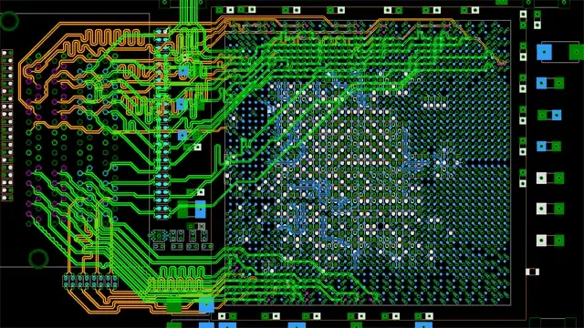
Microchips rank among the world’s most intricate devices, and the engineering methodologies behind them are equally sophisticated, involving the precise placement of billions of components to achieve targeted functions. Furthermore, testing is a frequently underestimated aspect of semiconductor development – a vital phase that must begin long before a physical prototype is manufactured, due to the immense scale and complexity of modern chips
1. Understanding DFT
Ensuring that each microchip leaving foundry is fully operational is of utmost importance, particularly because these components are often integrated into critical applications like medical equipment, automobiles, or aerospace systems, where malfunctions could lead to fatal outcomes.
In addition to identifying defective chips, it is also important to determine the underlying reasons for the failures and, whenever feasible, mitigate or completely eradicate them. To accomplish this, merely relying on exhaustive brute-force testing for every single function on every chip is inadequate – and practically impossible given the astronomical time constraints. Therefore, integrated circuits must be architected from the outset with testability as a core objective, an approach known as design for test (DFT).
By implementing DFT, engineers can optimize chip architectures for fast and effective testing using predefined patterns. This approach accelerates the verification cycle for each chip and simplifies root-cause analysis for any defects, while also generating high-quality data to train advanced machine learning models.
While DFT offers significant benefits, it also comes with a toll on physical chip design. Embedding test circuits consumes valuable space that could otherwise be used for processing power, memory, or other critical features. However, skipping verification is simply not an option. Therefore, DFT requires a delicate balance: minimizing the testing logic while ensuring comprehensive validation of the chip’s performance. This complex optimization problem makes it the perfect candidate for AI.
Read more on how DFT pre-silicon validation for a design: Tessent SiliconInsight: A Comprehensive Solution for IC Debugging and Testing
2. How AI drives technological progress
To explain, tools like Tessent leverage AI in two primary areas: hierarchical DFT and what he calls “analytical AI,” which is integrated into Siemens’ Streaming Scan Network (SSN) platform.
Hierarchical DFT was introduced to manage the ever-increasing size of chip designs. Instead of optimizing a test pattern for the entire chip at once, engineers optimize on a per-core basis, later aggregating these local results to build the final test protocol.
Even when AI is used to enhance hierarchical DFT – such as optimizing bandwidth or embedded compression – efficiency gains plateaued at a 20% to 30% reduction in pattern size. While significant, this improvement could not keep pace with the explosive growth of modern semiconductor designs. Recognizing this bottleneck, We have to take a radically different approach, leading to the development of analytical AI.
Instead of feeding test data directly to each core, SSN packetizes the information before transmission. This enables system-level optimization of data delivery across the entire chip. As a result, it reduces the required number of I/O test pins and internal test circuits, allowing all cores to be tested simultaneously.
Creating these packetized data streams is a complex task perfectly suited for analytical AI. By offloading this burden, designers can focus purely on optimizing their cores and defining basic test patterns. The SSN’s embedded AI handles the rest, automatically generating a highly efficient, packetized test suite without the need for heavy manual effort.
3. The future of chip verification
Testing might not be the most glamorous stage of engineering, but it is undeniably critical in the semiconductor industry. Faced with strict quality standards, massive datasets, and countless variables, the verification phase is ripe for AI disruption, achieving efficiency levels far beyond traditional methods.
As semiconductor architectures grow increasingly complex, adopting advanced technology is no longer optional. Moving forward, AI will serve as a vital enabler in both designing and rigorously testing the microchips of tomorrow.
(Source: Siemens)
Read more:
Contact us for free and detailed advice: