


The use of flexible printed circuit boards (Flex PCBs) and rigid-flex circuits has grown rapidly, primarily driven by the trend toward miniaturized electronic devices. However, due to their thin and bendable material properties, flex PCBs are much more fragile than standard FR4 rigid boards. This leads to higher defect rates during manufacturing, significantly driving up production costs.
To solve this problem, applying DFM (Design for Manufacturing) analysis to flexible circuits is a necessary process.
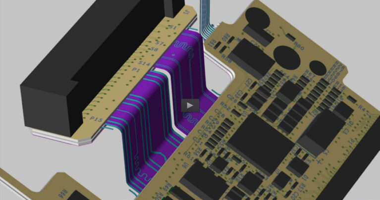
Figure 1. Flexible circuits pose new challenges compared to rigid circuits, such as bending and flexing capabilities.
1. 10 Manufacturing Barriers for Flex/Rigid-Flex Circuits
The biggest difference between flex and rigid circuits lies in their thermal expansion characteristics and copper adhesion. Below are the 10 most common manufacturing risks for flexible PCBs and how to address them.
1.1. Mounting SMT Components on Flexible Materials
Surface mount technology (SMT) components can be placed on flexible circuits by selectively using bonded stiffeners where needed. Copper on a flexible substrate is more prone to delamination than on a standard rigid board. Therefore, surface mount pads require additional support, typically by using a coverlay that partially overlaps the pads and vias.
Larger solder pads can also be used instead of a coverlay, providing a larger surface area for adhesion. However, using a combination of both support methods will create a pad with the best possible adhesion.
1.2. Making Solder Pads Larger Than Coverlay Openings
Designing solder pads larger than the access holes in the coverlay can significantly increase bond strength while reducing the likelihood of delamination.
This technique is similar to Solder Mask Defined (SMD) pad design for rigid boards. For designs that must bend, the coverlay provides additional anchoring to the copper features.
1.3. Trace Spacing in Bend Areas
The bend area is another region that requires extremely careful design. A general rule of thumb for trace spacing is to maintain 5 mm between the rigid circuit section and the bend area of the flex circuit (Figure 2). Bends located closer to the rigid board area than this distance are much more prone to fracturing.
Furthermore, without proper spacing, the coverlay located just beneath the rigid circuit area can peel off, exposing the copper layer.
1.4. Trace Routing Angles at Bend Points
There is a risk issue in bend areas regarding trace routing direction. The reliability and quality of flex circuits can be improved by ensuring that traces enter the bend area with little to no change in direction (Figure 2).
If changing the direction of traces within a bend is unavoidable, use rounded curves instead of sharp angled lines to reduce the likelihood of trace fracturing.
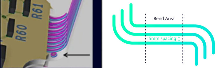
Figure 2. Trace spacing must be 5 mm between the rigid circuit and the bend section.
1.5. Trace Width
Conductor width is also particularly important. A safe rule of thumb is to design trace widths to be at least five times their thickness. Our recommendation is to use the thinnest copper trace possible to safely transmit the intended signal, and then adjust the trace width accordingly.
1.6. Plane hatching
Stress at bend points can be alleviated using a technique called plane hatching. Although a honeycomb (hexagonal) shape is the most effective at reducing angular stress, generally, any hatched pattern will provide better stress reduction compared to solid copper pours.
1.7. Adding Teardrops to Improve Durability
Teardrops (fillets) help improve the yield and durability of flex circuits. They are used in cases where the diameter of the solder pad exceeds the width of the trace connecting to it.
You should also avoid sharp angles at the junction between traces and pads to minimize stress concentration at the joint.
1.8. Transition Zones
Typically, this transition zone extends about 1.2 mm from the edge of the rigid circuit into the bend area to form a combined connection area of 2.5 mm.
This transition zone can be more fragile than the rest of the design, requiring special design considerations. Specifically, this includes avoiding the placement of vias, mounting holes, slots, or plated through-holes (PTH) near the junction of the flex and rigid sections. Additionally, the angle at which traces enter the rigid sections must not be 90 degrees.
1.9. Loosening Manufacturing Tolerances
Manufacturing tolerances for flex circuits must be loosened compared to rigid boards. The materials and construction techniques used in flex circuits can shrink, expand, stretch, and compress in ways that are entirely different from rigid boards. Loosening tolerances creates a safety margin that allows these physical phenomena to occur.
1.10. Thermal Expansion
Most adhesive-based flexible substrate materials are unfilled, which can lead to uncontrolled Z-axis thermal expansion. This condition makes vias and other features highly susceptible to delamination. It will also cause intermittent connections after components are soldered onto the flexible material surface.
To overcome this, components soldered on flex circuits require a much more robust solder pad design than those on rigid board areas.
Read more: Sat Nusapersada Increases Efficiency by 33% Using Valor Process Preparation
2. The DFM Solution for Flex Circuits: Valor NPI
Flex and rigid-flex circuit designs are becoming increasingly popular with the miniaturization of technology and the explosion of wearable devices. PCB layouts involving flex circuits require specific manufacturing processes. To ensure and optimize these designs for production, a dedicated DFM solution combined with a comprehensive, intelligent manufacturing model is the best tool to improve yield, save costs, and increase reliability.

DFM Analysis in Flexible PCB Design with Valor NPI
Valor NPI is a solution that integrates manufacturing knowledge into the application to provide expertise when running DFM analysis on PCB designs. Valor NPI offers complete DFM inspection coverage for rigid boards, flex boards, as well as the interconnections between them
Valor NPI can automatically identify issues related to the 10 barriers mentioned above and many other challenges. Identifying and fixing errors from the very beginning can save time, costs, and most importantly, prevent redesigns caused by manufacturing defects.
Flex circuits are harder to manufacture than rigid ones, and the best way to ensure designs are practically manufacturable is to run DFM checks continuously throughout the layout process, as well as running DFM during the final manufacturing release process.
Running DFM checks on PCB designs with Valor NPI can help reduce drawing revisions (respins) by an average of 57%. For rigid/flex circuits, ensuring manufacturability before sending model data to the fabricator is extremely crucial.
Applying DFM to PCB design helps save design time and reduces time spent fixing errors. Contact VBTECH today for direct consultation on solutions tailored to your business needs