


In product development and engineering, DFM and DFA are two frequently discussed concepts.
-
DFM (Design for Manufacturing)
-
DFA (Design for Assembly)
While both share the ultimate goal of making product realization easier, their core focuses differ significantly. In this article, VBTECH will break down these differences and explore how DFM and DFA apply to the PCB manufacturing process.
1. The Relationship Between PCB Design and DFM
In PCB design, DFM acts as a catalyst to improve bare board fabrication. It influences early decisions regarding trace width, layer stack-up, standard material usage, and the selection of manufacturing technologies to keep the fabrication process as streamlined as possible.
For instance, right from the early stages, engineers must decide whether a design strictly requires Blind/Buried Vias, VIPPO (Via-in-Pad Plated Over) techniques, or if standard through-hole vias will suffice. These initial decisions directly impact both manufacturability and overall production costs.
2. The Relationship Between PCB Design and DFA
While DFM focuses on the bare board, DFA is the driving force behind improving the component mounting and assembly process. Proper DFA application ensures sufficient component clearance for pick-and-place machines to operate smoothly, while also leaving adequate room for future testing, inspection, or rework.
To achieve this, design engineers require highly accurate geometric data and component pin dimensions. The most critical factor is ensuring complete compatibility between the actual physical component and its footprint on the layout. The DFA process is most effective when utilizing software that allows you to directly import the Bill of Materials (BOM) into your design to run simulations, check 3D clearances, and analyze solderability before sending the design files to the factory.
3. Practical Methods
Today, the traditional mindset of “anything can be manufactured given enough time, budget, and resources” is no longer viable in a highly competitive landscape, especially when cost efficiency is a matter of survival.
3.1. Abandoning Outdated Design/Manufacturing Models
-
“Over the wall” approach: A siloed working method where there is little to no seamless communication between the design and manufacturing teams.
-
“Sign-off” after the fact: Waiting until the design documentation is completely finished before sending it to the factory for review and approval. If errors are discovered at this late stage, revisions are costly and cause significant project delays.
3.2. Adopting Concurrent Engineering and Shift-Left Strategies
-
Cross-departmental expertise synchronization: Modern design philosophy requires the involvement of all stakeholders right from the initial decision-making phase—from design engineers, component engineers, and test engineers to PCB manufacturing experts (MFG).
-
It is crucial to recognize that a brilliant PCB designer is not necessarily an expert in mass production, machine operation, or automated optical inspection. Therefore, integrating manufacturing expertise into the design phase is mandatory to ensure real-world feasibility.
-
As a general rule, 60% to 80% of a product’s final cost is determined by decisions made during the design phase. Therefore, it is imperative to address these manufacturing concerns as early as possible. You can visualize the product development lifecycle as a funnel: the further you move down the funnel (closer to the production stage), the narrower your window for optimization or making cost-effective changes becomes.
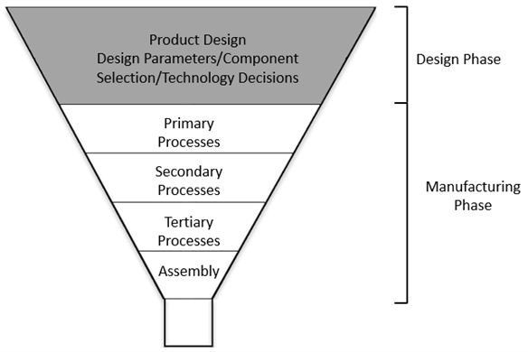
Product Development Cycle
With advanced DFM/DFA analysis software solutions from Siemens, detecting errors before production has never been easier. Contact VBTECH today for direct consultation on PCB design optimization solutions tailored to your business needs.